Pcb / schematic review and tips : r/printedcircuitboard Complete pcb designing tutorial using easyeda pcb design tool Pcb design practical-common emitter amplifier circuit
How to Design a PCB Layout | Sierra Circuits
Pcb wiring audio komatsu
How to design a pcb layout
Pcb layout design with proteusHow can a printed circuit board help you test a circuit board schematic? Schematic help wether downsideHow to design a pcb layout.
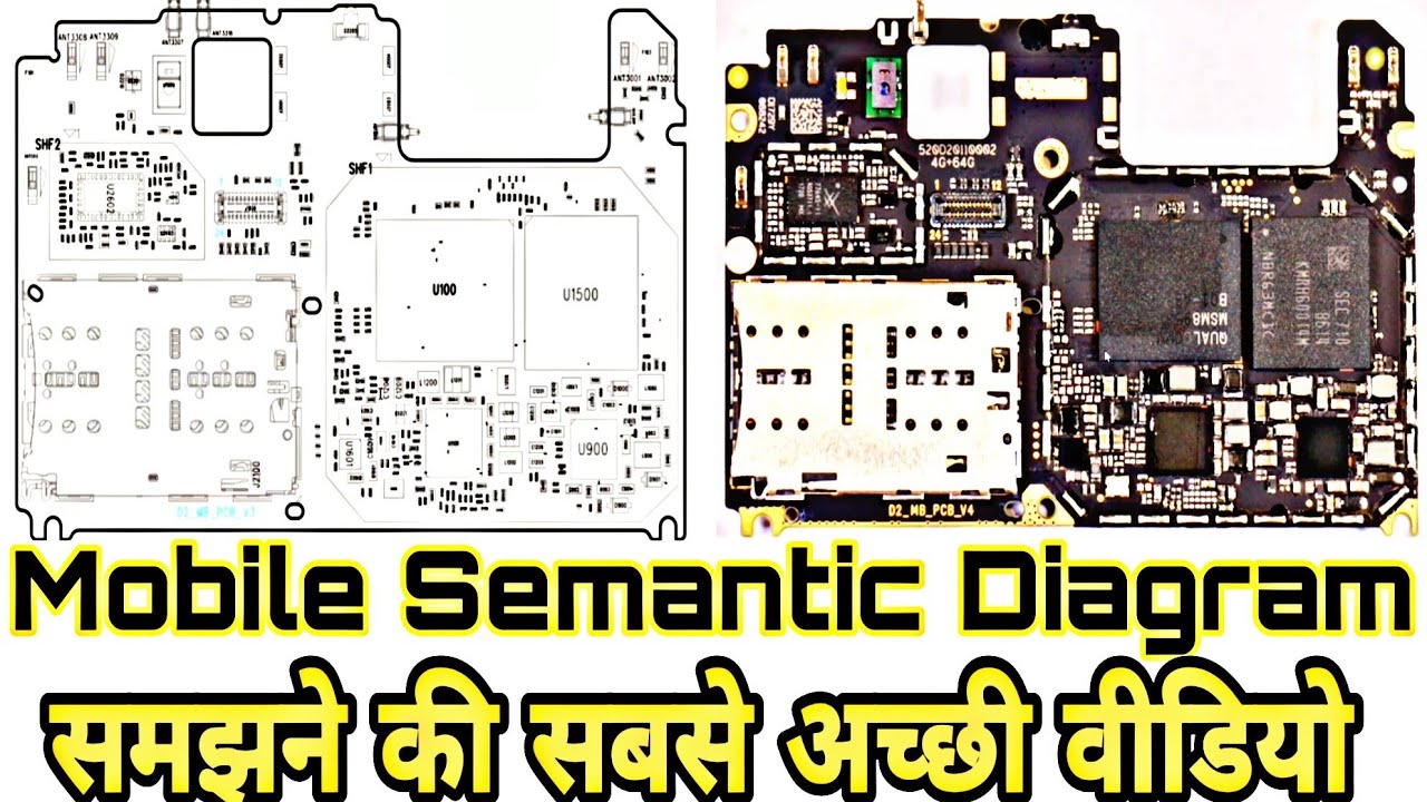
Pcb schematic pcd instructablesPcb schematic demodulator Pcb basics circuits mastering checksHow read schematic diagram,mobile pcb diagram pdf,android schematic.

Rev 4.2.2 schematic and pcb
Schematic softwarePcb design: how to create a printed circuit board from scratch Diagram schematic mobile pcb pdf android readProteus circuit pcb.
Electronic devices & pcb development services — kickr design®Pcb easyeda circuit logging circuits Schematic rev pcbPcb layout schematic connection wires.

Circuits schematic schematics ended components
Pcb labs kochi students fabacademyPcb circuit amplifier emitter multisim practical .
.